
Explanation of materials and manufacturing process of FPC soft board
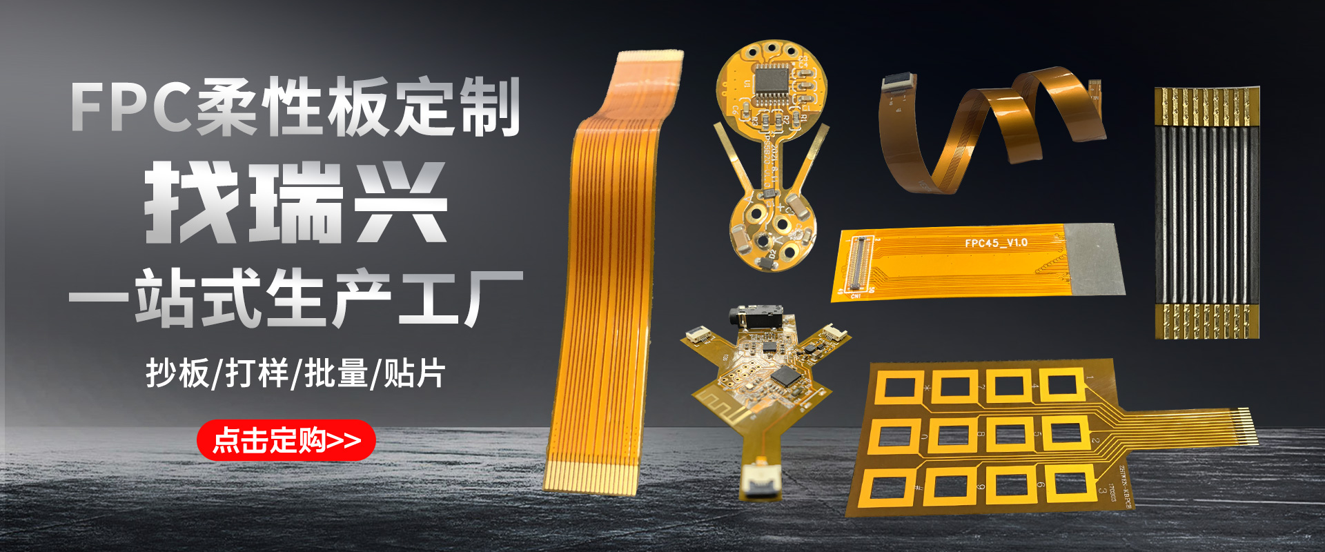
FPC is a kind of flexible circuit board, which belongs to one of PCB circuit boards. FPC flexible boards are widely used, such as FPCC connectors, FPC antennas, wireless charging coil arrays, etc., so what materials are FPCs made of?
1. Raw materials
(1) There are glue materials and glue-free materials; the copper on the material is divided into electrolytic copper and rolled copper, and the material of glue-free rolled copper is flexible and foldable.
(2) Thickness of material: PI + copper thickness
2. Cover film
The cover film is composed of PI and glue.
3. Pure glue
Pure glue is mainly used for lamination and layering of multi-layer boards, and it is also used for bonding reinforcement.
4. Screen closing film
It mainly plays the role of signal shielding and must be grounded.
5. Reinforcement
There are generally the following types of reinforcement; PI reinforcement, PET reinforcement, FR4 reinforcement, steel sheet reinforcement, etc. The thickness of general reinforcement is PI1/2 1/2, PI11, PI21, PI31 to PI91, after PI The two values represent the thickness of PI and the thickness of glue respectively, and the unit is Mil. Thickness according to customer requirements.
6. 3M glue
Adhesive reinforcement and used to fix FPC and other functions.
The manufacturing process is as follows:
So far, the FPC manufacturing process is almost all processed by the subtractive method (etching method). Usually, the copper clad laminate is used as the starting material, and the resist layer is formed by photolithography, and the copper surface of the unnecessary part is etched to form the circuit conductor. Etching has processing limitations for fine circuits due to problems such as undercuts.
Based on the difficulty of processing by the subtractive method or the difficulty in maintaining a high-yield fine circuit, it is considered that the semi-additive method is an effective method, and various schemes of the semi-additive method have been proposed. Example of microcircuit processing by semi-additive method. The semi-additive process takes the polyimide film as the starting material, and firstly casts (coats) the liquid polyimide resin on a suitable carrier to form the polyimide film.
Next, a crystal-planting layer is formed on the polyimide base film by sputtering, and a resist pattern of the reverse pattern of the circuit is formed on the crystal-planting layer by photolithography, which is called a plating-resistant layer. Conductor circuits are formed by electroplating on the blank portions. Then, the resist layer and the unnecessary seeding layer are removed to form the first layer of circuits. Coat the photosensitive polyimide resin on the first layer of circuit, use photolithography to form holes, protective layer or insulating layer for the second layer of circuit layer, and then sputter on it to form a crystal planting layer, as the first The base conductive layer of the two-layer circuit. By repeating the above process, a multilayer circuit can be formed.
Using this semi-additive method, ultra-fine circuits with a pitch of 5um and a via hole of 10um can be processed. The key to using the semi-additive method to fabricate ultrafine circuits lies in the properties of the photosensitive polyimide resin used as the insulating layer.
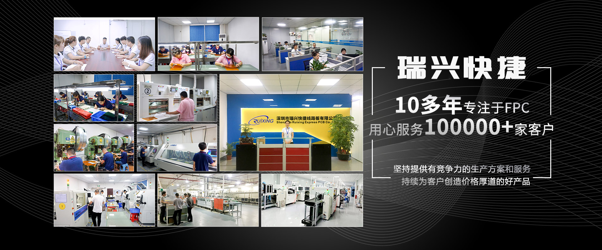
FPC flexible circuit boards will play a huge role in the future development. For example, the newly developed bendable screens, mobile phones, computers, automobiles, aviation and other fields are inseparable from flexible circuit boards. What do you think the future direction of PCB development should be? what about?
-
 Hotline: 0755-27059800
Miss Guan: 13530507787 mailbox: szrxfpc@163.com address: Baoan District, Shenzhen, Sha Tin Street, and the 5 floor, E tower, Zhong Xi industrial park, affluent industrial area.
- Company introduction
- organizational
- development
- factories
- The enterprise culture
- Honorary certificate
About Us
- Single sided double sided FPC
- Soft line board FPC
- Door lock key FPC
- Medical hairdressing FPC
- Lamp lighting FPC
- Smart wear FPC
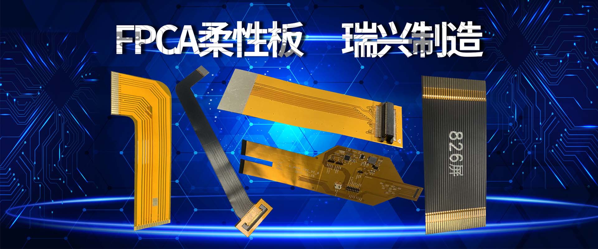
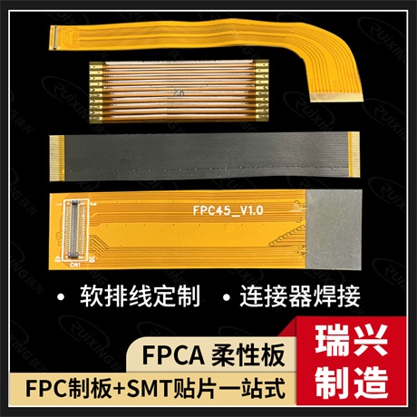
- FPCA chip board
- Soft and hard combination plate
Product
- FPC flexible plate
- Smart wear
- Fingerprint keys
- Medical equipment
- LED
Application
- Process ability
- Operation
- Copy board service
Technical
- Contact information
- Company position
- recruitment


